1956 Nobel Prize in Physics
Reason for Award
for their researches on semiconductors and their discovery of the transistor effect
Laureates
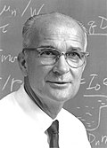
 United States of America

United States of America

United States of America
Explanation
A transistor is a tiny part that can turn a weak electrical signal into a strong one. Today, billions of these parts sit inside smartphones and game consoles. In 1956, Shockley, Bardeen, and Brattain discovered how the transistor works. They used a special material called a semiconductor, which is neither a metal nor an insulator. By carefully controlling the number of electrons moving through the semiconductor, they could stop or let electricity flow like a switch. Thanks to their discovery, we can build small, light computers and televisions.
Related Keywords
semiconductor
A semiconductor is a material whose electrical conductivity lies between that of conductors and insulators. Because its carrier concentration can be tuned by temperature, light, or doping, it is the core material for electronic devices. Silicon is the most common, but germanium and compound semiconductors like gallium arsenide are crucial for high-frequency applications. The size of the band gap determines a device’s operating temperature and emission wavelength. Transistors, solar cells, and LEDs are all practical implementations of semiconductor physics.
transistor effect
The transistor effect refers to the ability to control a large output current with a small input current or voltage inside a semiconductor. Specifically, a tiny base current modulates a much larger emitter-collector current, enabling gain. Because it operates at room temperature without relying on thermionic emission, it offers compactness and low power consumption compared with vacuum tubes. Achieving the effect requires high-quality pn junctions and low surface recombination velocities. In digital logic it acts as an on-off switch, while in analog circuits it provides signal amplification.
p–n junction
A p–n junction is formed by joining p-type and n-type semiconductors directly. Carriers diffuse across the boundary and create a charged depletion region. The internal electric field in this region rectifies current, allowing flow in one direction only. Applying bias voltage changes the depletion width, controlling the operation of transistors and diodes. Because incident light separates charges across the built-in voltage, the structure also underlies solar cells.
band gap
The band gap is the energy difference between the valence and conduction bands of a semiconductor. Carriers must gain at least this energy to transition from the valence band to the conduction band. A larger gap reduces leakage current at high temperatures, enhancing insulation. Conversely, materials with small gaps switch at low voltages and suit high-speed devices. In light-emitting diodes, the band-gap magnitude determines the emission color.
doping
Doping is the process of introducing trace impurity atoms into a semiconductor to control free carrier concentration. Group V elements such as phosphorus or arsenic donate electrons to create n-type regions, while group III elements like boron produce p-type regions. This can change resistivity by several orders of magnitude, steering current paths as designed. Ion implantation and diffusion are the main techniques used for precise doping profiles. Advanced doping control is essential for forming shallow pn junctions and ultrathin channels.
amplification
Amplification refers to the function of producing an output signal with larger voltage or current than the input. In a transistor, a small base signal controls a large collector current, providing a current gain β. Amplification is indispensable for high-frequency signals in radio communication and for volume control in audio equipment. Bandwidth, distortion, and noise figure are key metrics for amplifier performance. In integrated circuits, blocks such as differential amplifiers and operational amplifiers enable complex analog signal processing.
integrated circuit
An integrated circuit (IC) is an electronic circuit in which many transistors and passive elements are fabricated on a single semiconductor substrate. While the earliest ICs of the 1960s held only dozens of devices, modern chips contain hundreds of billions of transistors. This miniaturization has led to exponential improvements in computational power per unit energy. IC technology is embedded in virtually all electronic products including computers, smartphones, appliances, and automobiles. Clean-room environments, photolithography, and etching processes were developed specifically to realize ICs.
silicon
Silicon is the second most abundant element in Earth’s crust and the primary material of the semiconductor industry. High-purity single-crystal silicon is grown using the Czochralski or float-zone methods. Its 1.12 eV band gap strikes a balance between leakage current and carrier mobility for room-temperature operation. Silicon oxide provides excellent insulation and thermal stability, making it indispensable as the gate dielectric in MOSFETs. Silicon derivatives such as SiGe and SOI have recently been adopted for high-performance devices.
germanium
Germanium is an element used in the earliest transistor development and has a relatively small band gap of 0.66 eV. Bardeen and Brattain’s point-contact transistor was fabricated on a germanium crystal. Germanium possesses high electron and hole mobilities, making it suitable for high-speed devices and photodetectors. However, its thermal sensitivity and higher leakage led to its replacement by silicon. Recently, germanium’s optical absorption properties are being revisited in silicon photonics and tunnel FET research.
solid-state electronics
Solid-state electronics studies the behavior of electrons in solid materials and designs electronic devices accordingly. The invention of the transistor shifted the paradigm from vacuum-tube electronics to solid-state devices. The field employs quantum mechanics, statistical mechanics, and electromagnetism to analyze carrier transport and energy bands. Its evolution has dramatically increased information-processing power, enabling technologies like the Internet and artificial intelligence. Ongoing research into novel materials and nanoscale structures extends the discipline toward flexible electronics and quantum computers.