1973 Nobel Prize in Physics(1)
Reason for Award
for their experimental discoveries regarding tunneling phenomena in semiconductors and in superconductors, respectively (Phys. Rev. Lett. 5 (1960) 147-148; 464-466)
Laureates

 Japan
Japan
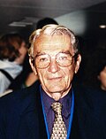
 United States of America
Explanation
1. Inside smartphones and game consoles are tiny roads for electricity called semiconductors. 2. Normally an electron cannot cross a wall, but if the wall is extremely thin, it can mysteriously slip through. 3. This is called the “tunneling effect,” named after cars passing through a mountain tunnel. 4. Dr. Esaki and Dr. Giaever were the first to show clearly that this strange effect really happens. 5. They stacked special materials like a sandwich and measured a faint current sneaking through the wall. 6. The phenomenon now powers computer memory, MRI scanners, and many other devices. 7. Our daily conveniences owe a lot to this tiny “electron tunnel.”
Related Keywords
quantum tunneling
Quantum tunneling is the probabilistic passage of particles such as electrons through a potential barrier that would be forbidden classically. The wavefunction decays exponentially inside the barrier, giving a finite transmission probability. The thinner the barrier, the larger the probability, becoming significant at the nanometer scale. Tunneling is critical not only in solid-state physics but also in alpha decay and stellar nuclear reactions. Experimental confirmation provides a cornerstone for quantum theory.
tunnel diode
Invented by Leo Esaki, the tunnel diode is a semiconductor device characterized by extremely high doping levels and an ultrathin depletion region. Under forward bias the current rises sharply and then enters a negative resistance region. It exhibits excellent high-frequency response, operating up to hundreds of GHz. It was used as a core device in oscillators and ultrafast switches. Today it survives in specialised circuits for education and instrumentation.
superconducting tunnel junction
A structure where two superconductors are separated by an insulating film, allowing Cooper pairs to tunnel quantum-mechanically. Differential conductance measurements reveal the superconducting gap and electron-phonon interactions. The device is applied as single-photon detectors and micro-coolers. It evolved into microwave-frequency qubit readout technology. Recently it is being developed as focal plane detectors for X-ray astronomy.
energy gap
An energy range in a solid where no electron states exist. In semiconductors it lies between the valence and conduction bands, determining electrical properties. In superconductors a gap opens near zero energy due to Cooper pair formation. Tunneling spectroscopy is a crucial method for measuring the gap directly. Variations of the gap with temperature or impurities are central topics in condensed-matter research.
negative differential resistance
A region in an I-V curve where increasing voltage leads to decreasing current. It is typical of tunnel diodes and Gunn diodes. Negative differential resistance enables self-oscillation and amplification. In high-frequency circuits it has been used as a compact oscillator source. The physical origin is the bias-dependent quantum-mechanical transmission probability.