2000 Nobel Prize in Physics(1)
Reason for Award
for basic work on information and communication technology (for developing semiconductor heterostructures used in high-speed and opto-electronics)
Laureates

 Russian Federation
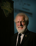
 Germany
Explanation
Inside cell phones and CD players are tiny parts that handle light and electricity. Mr. Alferov and Mr. Kroemer invented a “heterostructure,” a semiconductor that looks like a sandwich, to make those parts work faster and brighter. By stacking very thin layers of materials such as gallium arsenide, they created a super-smooth path for electrons so strong light can be made with little power. Thanks to this, we can talk to people far away and enjoy fast internet through optical fibers. The same idea is used in traffic-light LEDs and car brake lamps.
Related Keywords
semiconductor heterostructure
A multilayer stack of different semiconductor materials grown atom-by-atom; differences in band gap and lattice match are used to control electrons and photons. It forms the basis of high-speed transistors, laser diodes and quantum-well devices.
band gap
The energy difference between the valence and conduction bands that determines whether a material behaves as a conductor, semiconductor or insulator. In heterostructures, differing band gaps confine carriers and photons in desired layers.
gallium arsenide
GaAs is a direct-band-gap compound semiconductor with high electron mobility, suitable for high-frequency transistors and optoelectronic devices. Paired with AlGaAs it forms low-defect heterointerfaces.
heterojunction bipolar transistor
A bipolar transistor that uses a heterojunction to tailor the emitter barrier, delivering very high speed and gain. It is indispensable in microwave amplifiers for cellular base stations and satellite links.
semiconductor laser
A laser diode that emits light under electrical injection. Heterostructures allow low threshold currents and room-temperature CW operation, enabling optical-fiber communications and optical-disk technology.
quantum well
A low-dimensional structure where carriers are confined in a thin, lower-band-gap layer only a few nanometers thick. It is used to tune emission wavelengths precisely and to observe novel quantum-transport phenomena.
high-speed electronic device
A general term for transistors or rectifiers operating from gigahertz to terahertz ranges. High mobility and low transit time provided by heterostructures are key enablers.
optical fiber communication
Technology that transmits information as light through glass fibers. Heterostructure lasers and fast photodetectors enable high-capacity, low-loss long-distance links.