2010 Nobel Prize in Physics
Reason for Award
for groundbreaking experiments regarding the two-dimensional material graphene
Laureates
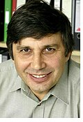
 Netherlands

 Russian Federation,
  United Kingdom of Great Britain and Northern Ireland
Explanation
If you keep peeling the grey carbon in a pencil lead with sticky tape, you can sometimes get a sheet only one atom thick. That sheet is called graphene. Although it is thinner than paper, graphene is stronger than steel and lets electricity flow very easily. Andre Geim and Konstantin Novoselov managed to lift this sheet with simple tape and showed how amazing it is. Their discovery may help us make bendable TVs, faster computers and other cool gadgets in the future.
Related Keywords
graphene
A one-atom-thick two-dimensional crystal in which carbon atoms form an sp²-bonded hexagonal lattice. It combines properties of metals and semiconductors; its charge carriers behave as massless Dirac fermions. Graphene exhibits extremely high room-temperature mobility, outstanding mechanical strength, extraordinary thermal conductivity and almost full optical transparency. It can be produced by mechanical exfoliation or CVD and is being explored for applications from RF electronics to composite reinforcement. The material is regarded as the starting point of modern two-dimensional materials science.
two-dimensional materials
A family of materials obtained by isolating single or few-atom layers from layered crystals. After graphene, compounds such as MoS₂, h-BN and WSe₂ have become major research targets. Because layers are bonded by van der Waals forces, in-plane and out-of-plane properties differ drastically. Parameters such as band gap, spin-orbit coupling and correlation strength can be tuned by layer number or twist angle. They are promising platforms for next-generation electronics and quantum devices.
Dirac cone
In graphene, valence and conduction bands cross linearly near the K points, forming a cone-shaped energy–momentum relation. This structure is mathematically identical to the massless Dirac equation, explaining why carriers move at about one-three-hundredth the speed of light. The cone leads to a half-integer shift in the integer quantum Hall effect and a Berry phase of π. Similar dispersions occur on topological-insulator surfaces and in Weyl semimetals. Research now focuses on gap engineering and flat-band formation to uncover new quantum phases.
carrier mobility
A measure (cm²/Vs) of how fast charge carriers move under an electric field of 1 V/cm. Graphene reaches tens of thousands cm²/Vs at room temperature, far exceeding silicon’s ~1400 cm²/Vs. The high value stems from low scattering and massless Dirac dispersion, enabling faster and lower-power devices. Mobility can be further enhanced by suppressing substrate disorder and phonon scattering. In ultra-clean samples ballistic transport and coherent quantum interference can persist even at ambient temperature.
ballistic transport
A regime where carriers traverse a channel without scattering from one end to the other. In graphene the mean free path can reach hundreds of nanometers at room temperature, enabling ballistic conditions inside nanoscale devices. Ballistic conductance appears in quantized steps of e²/h and exhibits reduced thermal noise, promising high-speed, low-noise components. It also provides a platform for cavity interference, electron lensing and other unique quantum phenomena. Encapsulation with h-BN or suspension increases the attainable mean free path.
van der Waals heterostructure
A multilayer stack of different two-dimensional crystals held together by van der Waals forces without breaking in-plane bonds. The absence of lattice-matching constraints enables high-quality quantum wells and superlattices fabricated at room temperature. One can engineer charge transfer, moiré potentials and interlayer tunnelling with great precision, leading to correlated insulators and flat-band superconductivity. Graphene often serves as an electrode or active layer and is integrated into optoelectronic and spintronic devices. Such heterostructures open avenues for material systems with functionalities beyond conventional three-dimensional semiconductors.